Reversing the PSR-70 hardware

First step in the actual reverse engineering is to start studying the PSR-70 hardware. This is quite service-friendly (meaning hacker-friendly) device: all circuit boards are single-sided and copper side silkscreen has IC numbers and jumper wire positions marked. There are also many useful looking signal names marked, like “D7”, “A12”, “IOWR” etc. It would be possible to draw the whole schematic from one high-quality photo of the circuit board.
My intention is not to draw the whole schematic, but at least the address maps should be figured out. It will make the interpretation of disassembly much easier. All address decoding is done with 7400-series discrete logic, no PAL-circuits or other nuisances used, this is very good.
Block diagram
Most of the electronics is on the large main board. The other cards are:
- Power + audio board contains the audio amplifiers, some kind of analog chorus-effect based on a BBD-circuit, power amplifiers feeding the speakers, and voltage regulation. The chorus effect is known in the front panel as “Stereo Symphonic”, and sounds quite nice.
- Front panel cards contain all the front panel buttons, leds and slide pots. The user interface contains over 70 push buttons, about 100 leds and a few slide pots. They are all on these two huge boards.
- Two or three smaller boards containing only front/back panel connectors.
This is the basic structure of the PSR-70:

Main board
The main board is the first thing to study because it contains all the essential functions. Its main components are:
- NEC D70008, a Z80 CPU
- EPROM 27256 (32 KB), contains the firmware
- TC5517 static 2 KB RAM, 4 pieces, which makes 8 KB of RAM together
- HD63A50 UART, handles the midi-interface
- 82C55 parallel I/O, handles scanning of the keyboard
- Several 74HC-series logic ICs, acting as glue logic for various things
- A couple of op amps handling the analog signals
This was the easy part: for all these, datasheets are available. More challenging part is a bunch of ICs which have text “Yamaha” stamped on and Google is very silent about them:
- YM3806 FM synthesizer chip. First hit from Google is titled “Undocumented sound chips”, which already tells the name of the game. After some more digging I could find some vague information that it should be a 4 operator 8 voice FM chip, probably same as YM3533, which does not help much, it is also unknown to everyone. Yamaha has special acronyms for all their chips, and this is “OPQ” (as in more widely known FM chips OPL, OPN etc.).
- YM2154 PCM rompler, producing the drum sounds. Yamaha acronym is RYP4 (Rhythm Processor #4). Somebody has done a pinout document about this but that’s about all.
- 2 pieces of YM2190 serial ROM. These are sample ROMs for RYP4 chip, containing drum samples. They use some Yamaha’s own serial bus when transferring data to RYP4.
- 2 pieces of YM3012 stereo-DAC. These ICs act as D/A converters for OPQ and RYP4 chips. They also use serial interface. Surprisingly, a proper Yamaha datasheet is available for these.
- A mysterious chip marked IG14330 which is even more unknown than the previous. By examining the PCB, it seems that the chip handles communication with the front panel boards using some kind of custom serial protocol. On the other side it is connected to CPU’s bus. I did not investigate this more, luckily understanding this IC is not critical for this reverse engineering project.
- A mysterious mask-ROM chip, no information available. By tracing the circuit board it is quite easy to conclude that this must be a 32 KB standard ROM on the CPU bus. And there is a silk screen marking “ROM2”. More about this chip later on.
Now I’m mainly interested in the OPQ and RYP4 circuits. Internet is clearly missing a documentation for these chips. Maybe I should try to fill in the gap.
OPQ is not so commonly used in Yamaha products. In addition to PSR-60/70 it has been used at least in CLP-100. There has been some investigation on CLP-100 by Achapee (?) but he has not gone to a level I want to go. A translation from his blog.
RYP4
is used in quite many Yamaha products. Of those, I own RX-15 drum machine, but
it has different sample ROMs than PSR-70. Here are some pictures of the RX-15 internals.
This photo shows the PSR-70 main board and its blocks. The next photo is the same board on the other side. The red markings are added by me.


Address decoders
By tracing from the photo and assisting with an ohm meter, I managed to draw this schematic about the memory address decoding circuitry.
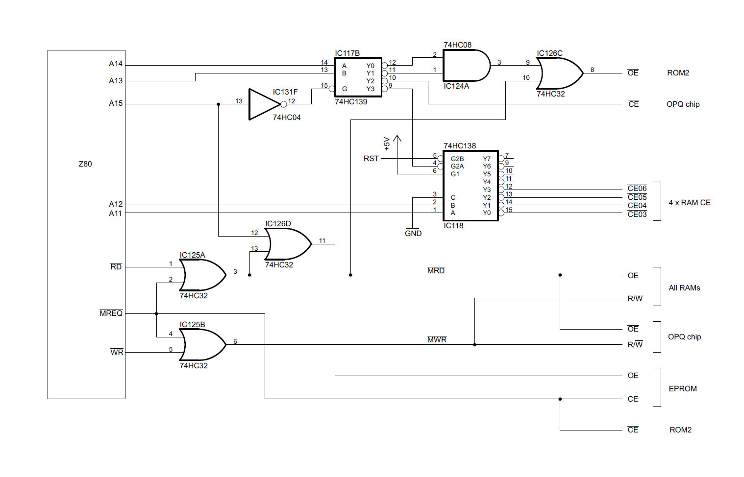
This is very basic demux/AND/OR decoder, it is easy to draw a memory map from that directly.
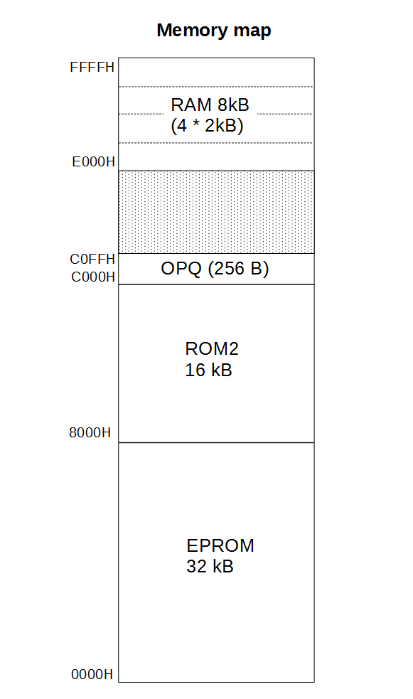
OPQ circuit is in the memory space although it is actually I/O. It is easy guess why: it uses 8 address lines, meaning it has 256 registers. If you placed it in the Z80 I/O address space, it would alone eat up the whole space. In this setup, it uses the memory addresses C000H...C0FFH.
And
then there is this mysterious ROM2. It has 16 KB of address space
reserved (8000H...BFFFH) but my conclusion was that it is a 32 KB
ROM. How come? What
is the role of ROM2? What does it contain if the software is in
EPROM? There is no need for large amounts of constant data. The drum
samples are already in separate chips communicating directly with
RYP4, there is no need to have any sample data here. All other imaginable mask ROM use cases are not needed in this keyboard.
Some more tracing from the board reveals that the highest address bit (A14) of the ROM2 comes from one I/O-pin of the 82C55. It means that the ROM2 is shown to processor in two 16 KB banks, and the bank can be switched using the 82C55 I/O-pin. All kinds of banking schemes were widely used during the history, but they all make using the ROM even more complicated.
I don’t understand the ROM2, I’ll leave it for now and start analyzing the I/O address decoding.
And after some more tracing I got this schematic about the I/O decoding:

This is again quite straightforward to convert to I/O address map:

There are four ICs in the I/O address space:
- UART in the addresses 10H and 11H
- 82C55 in 20H...23H
- The unknown IG14430 takes the addresses 30H...3FH. How many registers it really contains, I don’t know.
- RYP4 chip is in addresses 80H...FFH. It has 7 address lines and 128 registers.
Service manual
At this point, I was reading a conversation from the internet and someone mentioned the word “service manual”. This made me think that PSR-70 is so old that it might have such a manual available. Had not thought that before. After some googling around I found out that a service manual exists and is downloadable. It was quick to see that it is a very nice manual, among other things it contains a full schematic of the keyboard!
Now I got a bit pissed off. How could I be so stupid I did not check this first? I would have saved several hours of tracing the schemas from the circuit board. Seems I have lived too long in the modern world, where the service manuals of consumer equipment consist of one sentence: “If the device is not working, throw it away and buy a new one.” I was completely forgetting that in the 80’s decent service manuals were a common thing. This kind of omission won’t happen next time.
Anyway, the manual was useful still. It was nice to see that my reverse engineering was correct so far. And I had not yet done anything for the analog parts, now I don’t need to. And from the official schematic I could pick all kinds of smaller details which I had not noticed.
Here is the manual: https://elektrotanya.com/yamaha_psr-70_sm.pdf/download.html
Other notifications
Z80 contains in practice only one interrupt input (NMI is not very useful, not used here either). There is no interrupt controller but there are several interrupt sources: OPQ, RYP4, UART and IG13440. This has been solved with some glue logic on the board to combine the interrupts. This means also that the interrupt service routine must then do a polling round to find out who was requesting the interrupt.
In the Z80 interrupt input the scope shows a steady short pulse with 10 ms interval, which must be the real-time interrupt. Hard to say which circuit is sending it.
There are several crystal oscillators on the board: CPU is clocked at 6 MHz, OPQ uses 3,579 MHz and RYP4 2,25 MHz. UART gets (after some dividers) a 500 kHz baud clock. It is easy to guess that it uses internally divide-by-16 mode, which leads to speed of 31,25 kbit/s, which is the standard midi baud rate.
Analog board
Analog board from the component side:

Board has these functionalities:
- main mixer, mixing various audio outputs together
- VCA, implementing the volume control and mute
- chorus effect
- power amplifiers for speakers
- supply voltage regulation
This keyboard desperately tries to be stereophonic: it has two speakers and two audio outputs marked L and R. But the OPQ circuit cannot produce stereo output. Each voice channel can be directed to one or both of the two DAC outputs. You can pan the sound full left, full right or dead center. That's not much of a stereo. Even PSR-70 does not pretend it would be. The other output goes to chorus circuit, the other directly to main mixer, so you get a simple chorus on/off functionality. The only “stereo” is the chorus effect output.
Chorus effect is implemented with a MN3204 BBD chip, controlled by another Yamaha custom chip. This gets its control signals from RYP4, but the actual functionality is so far a bit unclear.
This is enough for the hardware, in the next post we’ll analyze the firmware.


Hi - in your poking at this synth, you didn't wind up with some spare IG14330 chips, did you? All signs point to that chip being fried in the one on my bench just now. No serial output, no G/L activity, 31KHz clock output instead of the 50KHz it's supposed to put out. All other inputs appear to be in order according to my logic analyzer.
ReplyDeleteHi. After this reverse engineering effort, I have built a midi sound module out of the PSR-70. Took the main and analog boards out, wrote a new software for the Z80 and put the whole thing in a table-top case. (Should actually write a blog post series about this project.)
DeleteThe only IG14330 I own is still sitting on the main board. To my understanding, it is not used for anything now, because the original front panel and keyboard are removed. And the new software does not use it. But desoldering it would mean dismantling the whole device. I'm not completely sure, whether the hardware would work without it. Most probably yes, but I'm a bit reluctant to try out, sorry.
Maybe you could try to find some "parts only" PSR-70 auction, probably there would be some other chip broken.
Cool - I'd love to read about it. I'm doing this for a lark, mostly to understand more about this discrete logic. Probably replace the IG14330 with an arduino emulating it. Rates are low enough. Getting a more and more marked up ROM listing as I try to sort out how the protocol.
Delete